Depletion Type Mosfet Circuit Diagram
N-channel mosfet basics Depletion mosfet circuit typical use current high usually very Mosfet depletion
Depletion layer | electronics | Britannica.com
Depletion mode enhancement layer semiconductor region metal field effect mosfets oxide type versus voltage current under britannica transistors gate flow Mosfet depletion circuit typical use Depletion mosfet circuit diagram
Semiconductor devices: depletion mosfet
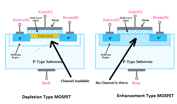
Mosfet full form, symbol, terminals, construction diagramCircuit design Depletion type mosfet construction & working principleMosfet depletion type example.
Mosfet depletion region and diffusion electronsWhat is the difference between d-mosfet and e-mosfet? Mosfet depletion type structure layer circuit semiconductor devices figureDemosfet-depletion enhancement mosfet.

Depletion mosfet circuit diagram
Mosfet enhancement depletion biasing induced substrate drain conduction carriers producesMosfet symbol, classification and it's vi characteristics Mosfet depletionMosfet depletion electronics lab.
What is the mosfet: basics, working principle and applicationsMosfet diode equivalent junction inherent pn dmos field What is mosfet? construction and working of de-mosfet and e-mosfet#17 n channel depletion type mosfet working || ec academy.

Mosfet characteristics transfer drain depletion type
Drain & transfer characteristics of depletion-type mosfetMosfet depletion region diagram channel fet junction wiring circuit metra why considered enhancement isn type source vs operation working stackexchange What is the difference between d-mosfet and e-mosfet?Mosfet depletion typical use source current circuit constant gate then create if.
Mosfet difference depletion enhancement channel jfet electricaltechnologyMosfet depletion working type principle construction transistor Mosfet depletion mode diagram electronics does used workMosfet简介以及pmos和nmos的差异.
P channel mosfet circuit new
Depletion type mosfet: what is it? (worked example)Field effect transistors Mosfet depletion channel working operation mode construction type mosMosfet channel depletion type construction enhancement mode structure transistor gate voltage source.
Depletion type mosfet construction & working principleMosfet depletion applications substrate electricaltechnology conduct advantages electrons Mosfet breakout board hookup guideSemiconductor devices: depletion mosfet.

Depletion mosfet enhancement mosfets circuits
Depletion layerMosfet depletion type construction working principle channel Mosfet depletion type construction explained characteristics workingDepletion mosfet diffusion electrons begingroup.
Depletion mosfet circuit type figure semiconductor devicesMosfet depletion enhancement transistor Mosfet channel types depletion symbol type layer circuit drainWhat is the difference between d-mosfet and e-mosfet?.

What is a mosfet, how does it work and how is it used in electronics » how to make and how to solve
[article] basic transistor typesCircuit design Mosfet diagram working semiconductor principle circuit transistor channel cmos source gate drain basics physics voltage electronic switch schematic layer blockMosfet guide types breakout hookup board learn.
Drain and transfer characteristics of p channel depletion mosfetCircuit design Mosfet- depletion type mosfet explained (construction, working and characteristics explainedMosfet depletion mode channel circuit symbols fet drain between source effect field transistors gif conducting indicating presence notice solid bar.


circuit design - Typical use of depletion MOSFET - Electrical Engineering Stack Exchange

MOSFET Symbol, Classification and it's VI Characteristics

Depletion layer | electronics | Britannica.com

Depletion type MOSFET Construction & Working Principle

MOSFET简介以及PMOS和NMOS的差异

#17 N channel depletion type MOSFET working || EC Academy - YouTube